OCTAVO
This project has run its course.
The code is still available.
If you have any questions, please contact me: eric@fpgacpu.ca or @elaforest
The Octavo soft-processor was my doctoral research project aimed at building
FPGA overlay architectures by increasing the performance of soft-processors
though adapting their architecture to FPGAs instead of ASICs. I continued it
after graduation to clean-up the code and implement the "Further Works" section
of the thesis. The work here spans from late 2010 to early 2019.
You can get the complete source from the Octavo GitHub Repository.
What Can Octavo Do?
- Run at ~80% of the absolute maximum possible clock frequency of an FPGA
design. This is about 2x the clock frequency of other soft-processors.
- Complete an instruction every clock cycle (CPI of 1.00), unless it's
blocked on I/O.
- Execute 8 independent, shared-memory threads in deteministic round-robin
order, as if they were each a separate CPU.
- Combines register file and local scratchpad memory. Each thread has the
equivalent of 256 registers and all threads share a pool of 1024 instructions.
All memory is 36 bits wide.
- Each instruction can read up to 2 local memory or I/O locations, and write
up to 2 local memory or I/O location per clock cycle, and automatically retries
if any I/O is not ready, without affecting other threads. This also applies to
any attached accelerator logic, as if they were ordinary registers.
- Each of these local memory accesses can be indirected through independent
zero-cycle pointers with automatic post-incrementing with strides of up to
+/-16 words.
- All branches execute in zero cycles, in parallel with an instruction, and
multiple branches can be tested in parallel in priority order. Each branch can
test one of 256 conditions combining all integer signed and unsigned
comparisons, sentinel values, counters, bitmasks, and external events.
- Each thread executes an independent subset of 16 instruction opcodes out of
over a million defined opcodes. Each thread can alter its opcode subset at
runtime.
- The ALU can perform some combination of the following in each instruction:
an addition/subtraction, any 2-term Boolean operation, any 3-term Boolean
operation with the result of a previous instruction, arithmetic/logical shift
left/right by one, move 2 inputs and outputs at once with optional bit masking
or swapping.
Project Outcomes
Increasing the performance of a soft-processor would allow moving more of an
FPGA design into software, and reduce the number of time-consuming hardware
re-spins. It should also simplify the design of both the hardware and software:
- The software can do more work with simpler code, without loop unrolling or
vectorization, and where performance demands it merely passes data to
accelerator hardware.
- The hardware doesn't have to deal with control or other irregular
computations. An accelerator is a simple pipeline. This also makes meeting
timing on a high clock frequency trivial.
Unfortunately, it's possible to overshoot these goals and end up with a
system where the software is harder to write than the hardware. Octavo can do
up to 4x as much work than any conventional scalar soft-processor (as little as
half as many cycles on twice as fast a clock), but this comes at the cost of
code which is either too hard to reliably write manually, or requires complex
software to assist the programmer, and it must be split across 8 threads.
For example, the assembler I wrote to support enough of Octavo to write
micro-benchmarks is 2160 lines of Python implementing 35 classes, and has
multiple phases (parsing, data and code allocation, data dependency resolution
and code generation, and binary images generation). It resembles more a crude
compiler. In hindsight, this complexity is inevitable since managing the
configuration and allocation of the opcodes, branching logic, pointer logic,
and ALU state all boils down to a problem of calculating register allocations,
initialization data, variable lifetimes, and code hoisting (even if the
programmer can easily do that last one).
The software complexity problem propagates upwards too. Since Octavo's
hardware is so different, there is no existing C compiler that can support it,
and although possible, it would be a whole separate project to add support to
GCC or LLVM. Without C support, connecting Octavo to existing software systems
becomes a manual, tedious process, cancelling out the simplified hardware
design process.
Briefly put, too much of the design difficulty had been transferred to the
software. It would now be less design effort to gain performance by adding
accelerator pipelines tightly-coupled (i.e.: not hanging off a bus or
interconnect) to a (mostly) conventional soft-processor with compiler support.
Multithreading, Accelerators, and Performance Limits
Can we transfer what was learned from Octavo to conventional
soft-processors, and is it worth doing so? Let's consider a few possible cases
and estimate the performance gains that are theoretically possible.
Our baseline for comparison is a conventional scalar RISC soft-processor
which runs 1 thread, at 1x clock frequency, and has a CPI of 1.3. (This is a
slightly optimistic ballpark value for a good scalar RISC design executing
general-purpose code.) At the other end, we have Octavo v3 which runs 8
threads, at 2x the clock frequency, and has a CPI of 1.0.
From Octavo's reduced CPI and increased clock frequency we can calculate
that, all other things being equal, Octavo has 2.6x the performance of the
scalar soft-processor. In reality, the difference can be as much as 4x, so
there's up to a 1.54x (i.e.: about 2/3rd as many instructions) reduction in
Octavo's executed instruction count also, which sounds about right (e.g.:
roughly -25% for branches now being zero-cycle, and another -10% for zero-cycle
pointers and other little ALU tricks).
The first obvious step is to convert the scalar soft-processor to a
round-robin multithreaded design, which runs 8 threads, at 2x the clock
frequency, a CPI of 1.0, and no change in instruction count. Having eight
threads is merely a convenient power of two and matches a likely number of
stages for the pipeline. Plus, any number of threads greater than one already
brings in the same programming complications. The longer pipeline and
round-robin multithreading means the usual pipeline stalls from branches won't
happen, those from loads are minimized, and the ALU result feedback paths are
no longer necessary, simplifying the pipeline and granting the 2x clock
frequency increase (about as much as physically possible) and dropping CPI to
1.0.
From the clock frequency and CPI changes, we can estimate a 2.6x increase in
performance, if you can use all threads. The design of accelerators is also
improved, since we now have 8 cycles to perform any computation (at 2x clock
frequency) before returning a result to a thread after one thread instruction
of latency. The same applies to memory accesses. If your application is already
parallel, multithreading a scalar soft-processor is a definite improvement: the
code is unchanged, your software runs up to 2.6x faster, on less area than 2 or
3 scalar CPUs, and any accelerator you add has its performance potentially
doubled (assuming everything runs on the same clock).
However, since even in simple cases an application accelerator attached to a
RISC scalar soft-processor grants speedups of many orders of magnitude, all
this effort for a 2.6x speedup in software doesn't seem worthwhile. It would be
better to keep the software very simple, compatible, in charge of the control
and other irregular computations, and move the heavy, repetitive, regular
computations to an accelerator. Both hardware and software design effort are
reduced this way.
Remaining Ideas
Other than round-robin multithreading a sufficiently long pipeline to
maximize clock frequency, there are still some design ideas in Octavo which
would benefit conventional scalar CPUs, without complicating the software in
incompatible ways:
Accelerators Connected To Registers
Transferring data to/from an accelerator through loads/stores is simple, but
since many functions take at least two arguments and return one, loads/stores
are a bottleneck. If there was an way to pass the contents of the source and
destination registers of an instruction directly to an accelerator, even if the
destination register gets its result several cycles later, we could keep
accelerators busier and interface with them with less overhead. It would make
using smaller accelerators worthwhile, giving a finer breakdown of the work
that is less dependent on the exact application being accelerated (i.e: a
smaller semantic gap).
Loading/Storing Two Words At A Time
Similarly, at the limit where data is not reused internally either due to
simple code or an already hardware-accelerated computation, the memory access
stage poses a bottleneck causing all computation tends towards the form "load,
load, compute, store". To reduce this overhead, we would need dual and parallel
memory pipeline stages to queue up (and overlap) two ordinary load and/or store
instructions. A dual write port register file would allow dual loads to
complete in one cycle rather than consecutively, but unless the memory latency
is very small, simply overlapping otherwise consecutive memory latencies will
have a greater benefit. Dual write ports on
FPGAs are also costly in area and in speed.
Clock frequency, Area, and Portability
Although Octavo (v1 and v2) was originally aimed at Altera's Stratix IV
FPGA, it performs pretty well on other Altera devices. It generally runs twice
as fast as a NiosII/f, and gets fairly close to the absolute upper clock
frequency limit allowed by the FPGA hardware.
Octavo v2 Fmax on Various Altera Devices (tuned to Stratix IV)
| Family | Device | Average | Maximum | Avg/Max | Limit | Max/Lim |
| | | (MHz) | (MHz) | (Ratio) | (MHz) | (Ratio) |
| Stratix V | 5SGXEA7N2F45C1 | 508 | 588 | 0.864 | 675 | 0.871 |
| Stratix IV | EP4S100G5H40I1 | 470 | 493 | 0.953 | 550 | 0.896 |
| Arria V | 5AGXFB5K4F40I3 | 272 | 300 | 0.907 | 400 | 0.750 |
| Cyclone V | 5CGXFC7D6F31C6 | 239 | 267 | 0.895 | 315 | 0.848 |
| Cyclone IV | EP4CGX30CF19C6 | 187 | 197 | 0.949 | 315 | 0.625 |
The Fmax of Octavo v3 is 5% lower than Octavo v2, but operates
with less overhead and a more powerful ISA. On an Intel Cyclone V
(5CGXFC5C6F27C7), an Octavo v3 instance with Multiplier and Accumulator
accelerators uses 2245 ALMs (1808 LUTs and 4854 flip-flops), 12 M10K Block
RAMs, 4 DSP blocks, and runs at up to 222 MHz (out of a max possible of 275
MHz). You could fit about 10 such Octavo instances on this FPGA.
The critical path is the calculation of flags between the ALU and the
Branching Modules, which architecturally could not be pipelined, else they
would fall out of sync with the current thread or introduce a second clock
cycle of latency on branches, which is unacceptable. However, since this
critical path is fixed, and all the other configurable parts of Octavo are
heavily pipelined, we can increase the number of Branching and Address Modules,
and the number of I/O ports, with little to no reduction in clock frequency.
Since Octavo v3, the design should be quite portable to other FPGAs (Xilinx,
Lattice, etc...) since it uses no vendor-specific modules and is heavily
pipelined. Any vendor-specific hardware can be attached as an accelerator,
without altering Octavo's ISA or architecture.
Design Evolution
Octavo v1
") The first version of Octavo, published in 2012, was a proof-of-concept: can
we maximize operating frequency and issue one instruction per cycle? Octavo v1
had Instruction (I) and Data (A and B) memories, a simple controller (CTL)
which could execute a branch based on the contents of a memory location in A,
and an ALU which could do addition, subtraction, multiplications, and basic
Boolean operations. It reached the 550 MHz limit of the Stratix IV FPGA, but
had limitations: you had to write self-modifying code to implement
indirect memory accesses, and the ALU was idle during a branch.
The first version of Octavo, published in 2012, was a proof-of-concept: can
we maximize operating frequency and issue one instruction per cycle? Octavo v1
had Instruction (I) and Data (A and B) memories, a simple controller (CTL)
which could execute a branch based on the contents of a memory location in A,
and an ALU which could do addition, subtraction, multiplications, and basic
Boolean operations. It reached the 550 MHz limit of the Stratix IV FPGA, but
had limitations: you had to write self-modifying code to implement
indirect memory accesses, and the ALU was idle during a branch.
Octavo v2
") The second version of Octavo, published in 2014, addressed the
inefficiencies of the first version. Octavo v2 keeps the same ALU, and the
same Instruction (I) and Data (A and B) memories, but adds a Branch Trigger
Module (BTM) which calculates one or more branches in parallel with the current
instruction based on the result of the previous instruction. Branches take zero
cycles in the common case. The Address Offset Module (AOM) can alter the
instruction operands before execution to implement indirect memory access with
post-incrementing. Finally, the I/O Predication Module (PRD) manages the I/O
ports: if an instruction operand refers to a port which is not ready, the
instruction is forced to a no-op and the Controller (CTL) re-fetches the same
instruction to retry again. Octavo v2 no longer reached the maximum possible
operating frequency, but its improved efficiency more than made up for the
loss. Octavo v2 could also be operated in a SIMD configuration, with up to 32
datapaths.
The second version of Octavo, published in 2014, addressed the
inefficiencies of the first version. Octavo v2 keeps the same ALU, and the
same Instruction (I) and Data (A and B) memories, but adds a Branch Trigger
Module (BTM) which calculates one or more branches in parallel with the current
instruction based on the result of the previous instruction. Branches take zero
cycles in the common case. The Address Offset Module (AOM) can alter the
instruction operands before execution to implement indirect memory access with
post-incrementing. Finally, the I/O Predication Module (PRD) manages the I/O
ports: if an instruction operand refers to a port which is not ready, the
instruction is forced to a no-op and the Controller (CTL) re-fetches the same
instruction to retry again. Octavo v2 no longer reached the maximum possible
operating frequency, but its improved efficiency more than made up for the
loss. Octavo v2 could also be operated in a SIMD configuration, with up to 32
datapaths.
Octavo v3
") The third version of Octavo, completed in 2019, fixes some
limitations of Octavo v2 which was written in a hurry. The codebase was
cleaned up, and computational overhead further reduced: multi-way branching with priority arbitration over
200+ branch conditions (FC),
more flexible indirect addressing (AD), a Literal Pool to
reduce duplication in Data memories (DM), a programmable Opcode Decoder (OD), a
new three-operand ALU which supports bitwise parallelism and instruction
chaining, and a new addressing mode to move twice as much data per instruction
when data movement dominates computation (AS).
The third version of Octavo, completed in 2019, fixes some
limitations of Octavo v2 which was written in a hurry. The codebase was
cleaned up, and computational overhead further reduced: multi-way branching with priority arbitration over
200+ branch conditions (FC),
more flexible indirect addressing (AD), a Literal Pool to
reduce duplication in Data memories (DM), a programmable Opcode Decoder (OD), a
new three-operand ALU which supports bitwise parallelism and instruction
chaining, and a new addressing mode to move twice as much data per instruction
when data movement dominates computation (AS).
Octavo v3 Architecture
The following block diagrams detail the implementation of Octavo v3. They
are not exact schematics, as some address translation and decoding logic is
omitted for clarity, but primarily serve as an architectural reference, and
make clear the number of pipeline stages a path traverses, which is crucial to
get exactly right else threads will corrupt each other.
Each diagram is divided by numbered vertical dashed lines which denote
pipeline registers. Each module spanning multiple pipeline stages has its
blocks numbered, which match the pipeline register numbers in the detailed
block diagram for that module, and so on... Each line represents a single bit
or a bus and is named so it can be referenced in sub-diagrams. Small, unnamed
boxes with a chevron at the bottom denote registers without logic. Larger such
boxes denote synchronous memories. There are no asynchronous memories in
Octavo.
You can click on a diagram to get a high-resolution version.
Instruction Format
Octavo's has only two 36-bit instruction formats: common and split.
A common instruction has, from the most-significant bits down (left to right), the following fields:
- A 4-bit opcode (OP), denoting one of 16 reconfigurable operations.
- A 12-bit destination operand (D), which contains the write address for the result of the instruction.
- A 10-bit source operand (A), which contains the read address for the Data Memory A.
- A 10-bit source operand (B), which contains the read address for the Data Memory B.
A split instruction divides D into two 6-bit fields DA and DB which each address the first 64 locations
of Data Memories A and B, respectively. Briefly put, split instructions can move two data items at once.
The configuration of an opcode (OP) defines if an instruction is split or common.
All instructions are conventional 3-operand instructions, where D = A
OP B for common format, and DA = A OPa B and
DB = A OPb B for the split format.
Memory Map
Octavo instructions operate only on its internal memories. External loads
and stores are done through I/O ports mapped into these memory spaces. There
are four 1024-word memory spaces:
- The Data Memory A, read by the 10-bit A instruction source operand.
- The Data Memory B, read by the 10-bit B instruction source operand.
- The Instruction Memory I, read by the 10-bit Program Counter (PC).
- The High Memory (H), which is not readable.
Except for H, each memory is independently mapped in a read range of 0-1023.
For writes, the 12-bit D instruction destination operand sees all four memories
consecutively mapped in a 0-4095 address space. Octavo's other internally
configurable memories and hardware are mapped in the H memory range 3071-4095.
A number of memory locations in the A and B Data Memories have special
functions memory-mapped onto them. Most have a configurable number of locations
and start addresses, so the following values are examples:
- Address zero always reads as zero and sinks writes.
- A contiguous range of locations (e.g. 0-31) are set as Shared Memory: all
threads access them using the same physical address. Addresses beyond this
range are automatically offset into each thread's private memory area.
- A contiguous range of locations (e.g. 24-27) are set as Indirect Memory:
accesses to these locations cause a per-thread programmable offset to be added
to the location's address before the read or write access, redirecting the
access to any other location in memory, like a pointer.
- A contiguous range of locations (e.g. 28-31) map to read and write I/O
ports. Accesses to these locations do not use the Data Memory, but instead read
or write from word-wide I/O ports with a ready/valid handshake (expressed using
enable signals and empty/full signals). If an I/O port is not ready, the
instruction is converted to a no-op ("Annuled") and re-tried the next time the
same thread comes around.
- The remaining Shared Memory locations (e.g. 0-23) are used as a literal
pool: constant numbers such as 0, -1, 1, bitmasks, etc... are stored here only
once and shared amongst all threads. Other numbers are stored in each thread's
private memory.
Data and Control Paths
 The top row of modules makes up Octavo's Control Path:
- A 6-stage Flow Control module (FC) produces a 10-bit Program Counter (PC) for each thread in round-robin order, and a Cancel (C) signal if a branch did not go as predicted and thus should cancel (turn into a no-op) the associated parallel instruction. C affects nearly all functions that follow. An instruction no-op'ed because of C is "Cancelled", and not retried.
- An Instruction Memory (IM) providing the 36-bit instruction, divided into a 4-bit opcode (OP), two 10-bit source operands and one 12-bit destination operand (A, B, and D, respectively). There are 1024 entries shared across all threads.
- An Opcode Decoder Memory (OD) which translates the opcode into Control Bits (CTL). There are 16 entries per thread (one per opcode), and 20 Control Bits per entry. Thus, 220 possible instructions.
- An Address Splitter (AS) which takes the 12-bit D operand and splits it into 6-bit DA and DB destination addresses (each with a constant upper 6 bits to match the address range of the A or B Data Memory) if the instruction uses the split addressing mode, else it simply duplicates D into DA and DB.
The bottom three rows make up Octavo's Data Path:
- The 2-stage I/O Predication module (PR) takes in the source and destination operands addresses (DA/DB/A/B) and the empty/full bits for the read and write ports (E/Fr and E/Fw), and produces a number of indicators:
- For each source operand, is_IOr signals that the address refers to a read I/O port.
- For each destination operand, is_IOw signals that the address refers to a write I/O port.
- If all the referenced I/O ports are ready to read/write, then an "I/O Ready" (IOR) is raised. Else it is kept low. IOR affects nearly all functions that follow. An instruction no-op'ed because of IOR is "Annulled", and will be retried the next time the same thread comes around, until the referenced I/O ports are ready.
- If any read I/O ports are accessed, then their corresponding read enable (rden) signals are raised to signal the other end that the data has been read in.
The remainder of the PR row simply carries IOR and C along the remainder of the pipeline. The next row does the same to CTL and other signals, and its last three stages are shown in dashed outline to indicate that these registers, although logically in these pipeline stages, were manually retimed further down to improve timing.
The bottom row contains the Addressing module (AS), the Data Memory module (DM), and the Arithmetic and Logic Unit (ALU):
- The 2-stage Addressing module (AD) takes the instruction operands (DA/DB/A/B) and separately adds one of three offsets to each of these operands to generate DA'/DB'/A'/B':
- Zero if the location is shared across all threads, such as the literal pool, the I/O ports, High Memory, and Instruction Memory.
- A Default Offset, unique to each thread, which divides the Data Memory amongst the threads.
- A Programmed Offset, unique to each thread and tied to specific fixed memory locations which act as pointers to any other location in memory.
- The 2-stage Data Memory (DM) internally has A and B RAMs read by the A' and B' operands, and written by the DA' and DB' operands (which are following alongside the ALU and will arrive with its results). The read and write I/O ports (I/Or and I/Ow) are memory-mapped to some locations in DM. If the operands refer to the I/O ports, they are accessed instead of the RAMs. The write enable (wren) signals are generated here to signify valid write I/O data.
- The 4-stage ALU takes in the pipelined CTL' control bits and the A and B outputs from the Data Memory and produces two results RA and RB, which then travel alongside the destination addresses DA' and DB'. The IOR, C, and DB' signals also run backwards through part of the ALU, which will be explained in the ALU's diagram.
Flow Control Module (FC)
 The Flow Control module (FC) computes the next Program Counter (PC) for each thread in turn, as well as if the current instruction must be cancelled (C) because a parallel branch did not go as predicted. The FC contains:
- One or more Branch Modules (BM) which each calculate a separate branch in parallel.
- The Branch Arbiter (BA), which receives the output of the BMs and selects the signals from the highest priority branch taken. The first BM has highest priority.
- The Controller (CTL) which takes the prioritized branch signals and outputs the Program Counter (PC) for the next instruction. The PC will point to the next instruction normally, or the branch destination if any, or the current instruction if it is Annulled by IOR and must be re-tried.
The new PC value is fed back to the BMs through 4 pipeline stages to synchronize it with the instruction fetched from that PC in the same thread. (FC pipeline stages 2 through 5 plus 4 feedback stages add up to 8 stages, one per thread).
Branch Module (BM)
 The 5-stage Branch Module (BM) takes in the result of the previous
instruction (Rp) as well as some Flags computed by the ALU from that
previous instruction. The result and destination address of the previous
instruction are also denoted as RB/DB' (identical to Rp) are also
used to configure the BM. The I/O Ready and Cancel signals from the previous
instruction (IORp and C (should have a sub-p there)) will prevent
any external updates or internal state changes from taking effect if the
previous instruction was no-op'ed. The BM also takes in the current I/O Ready
(IOR) to stop a branch from executing until the parallel instruction can
proceed, and the Program Counter (PC) value of the current instruction to
determine if a branch happens in parallel with it. The BM produces the
following signals:
The 5-stage Branch Module (BM) takes in the result of the previous
instruction (Rp) as well as some Flags computed by the ALU from that
previous instruction. The result and destination address of the previous
instruction are also denoted as RB/DB' (identical to Rp) are also
used to configure the BM. The I/O Ready and Cancel signals from the previous
instruction (IORp and C (should have a sub-p there)) will prevent
any external updates or internal state changes from taking effect if the
previous instruction was no-op'ed. The BM also takes in the current I/O Ready
(IOR) to stop a branch from executing until the parallel instruction can
proceed, and the Program Counter (PC) value of the current instruction to
determine if a branch happens in parallel with it. The BM produces the
following signals:
- Branch Reached (BR) when we arrive at an instruction with a parallel branch.
- Jump (J) is asserted if the branch is taken.
- Cancel (C) is asserted if the branch did not go as predicted and the parallel instruction should be turned into a no-op (and not re-tried).
- Branch Destination (BD) is the address to branch to if Jump is asserted.
The BM contains these sub-modules:
- The Branch Detector (BD), which checks if the configured branch conditions are met.
- Two Branch Sentinel (BS) modules, which each check the result of the previous instruction (Rp) against a set value, with bit masking.
- A Branch Counter (BC), which counts down by one each time a branch is reached (BR). It's output is fed back, after a synchronizing delay, to the BD to implement a branch when the BC reaches zero (or has not reached zero yet).
Branch Detector (BD)
 The 2-stage Branch Detector (BD) begins with a Branch Configuration Memory (BCM) which defines one branch for each thread. The branch configuration bits are:
- Branch Origin (BO), a 10-bit value specifying at which Program Counter (PC) value does the branch take effect.
- Branch Origin Enable (BOE), which if cleared has the branch take effect at any PC value, causing the branch to happen at any time when the conditions are met and acting like an exception.
- Branch Destination (BD), a 10-bit value specifying the new Program Counter (PC) value if the branch is taken.
- Branch Predict (BP), which specifies if the branch is predicted to be taken, or not.
- Branch Predict Enable (BPE), which can disable the BP if no branch prediction is necessary.
- Branch Condition (BC), an 8-bit value which defines which Flags (from the previous instruction result) must be true and/of false for the branch to be taken.
The BD calculates the following values:
- If the current instruction PC matches the BO, then the branch is reached (BR) and the next calculations are enabled.
- If the Condition Predicate module (CP) find that the Flags match the Branch Configuration (BC), then the Jump (J) signal is raised, signalling the branch is taken. If the previous instruction was Annulled (IORp is low), then recirculate J until the instruction is ready and retried. (We can't recompute the branch conditions if the previous instruction was a no-op and so doesn't generate the correct Flags.)
- If the output of the Condition Predicate (CP) module does not match the Branch Predict (BP) bit, then raise Cancel (C) to no-op the current instruction without re-trying it.
Condition Predicate (CP)
 The Condition Predicate module (CP) takes two 2-bit condition selectors and one 4-bit Boolean operation definition fed to a Universal Dyadic Boolean Operator and determines if the conditions are met. The CP design is discussed in detail here. The condition bits are mainly derived from the result of the previous instruction:
- Negative (N)
- Carry-Out (Co)
- Sentinel Value 1 (SV1p)
- External Input 1 (I1)
- Less-Than (N⊕V)
- Counter (CTRp)
- Sentinel Value 2 (SV2p)
- External Input 2 (I2).
Branch Sentinel (BS)
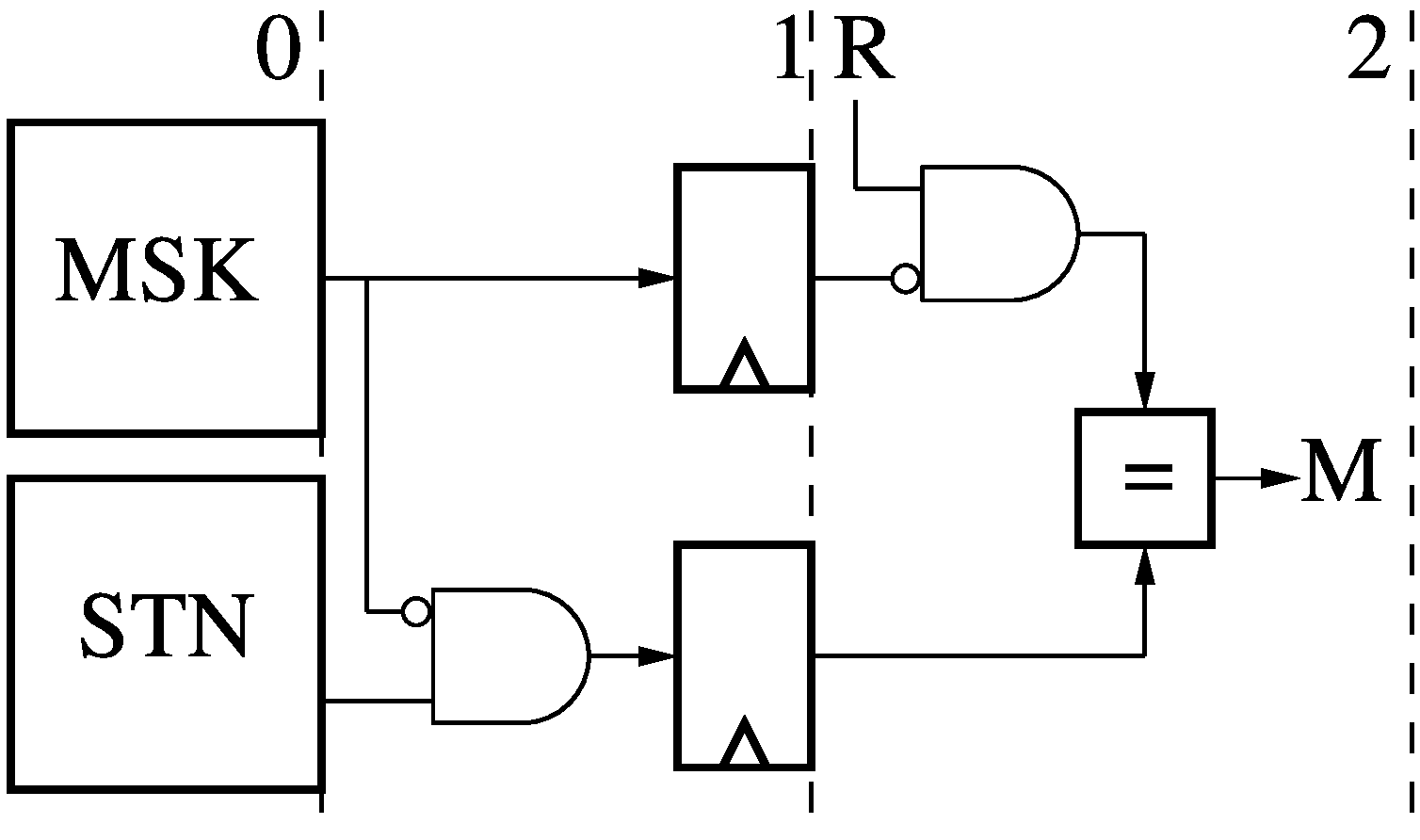 The 3-stage Branch Sentinel (BS) has two programmable memories, each holding
one value per thread: a Mask (MSK) and Sentinel (STN). The BS applies the Mask
to the Sentinel and to the result (R) of an instruction and then checks for a
match (M). Any bit position set to 1 in the Mask is omitted from comparison.
The 3-stage Branch Sentinel (BS) has two programmable memories, each holding
one value per thread: a Mask (MSK) and Sentinel (STN). The BS applies the Mask
to the Sentinel and to the result (R) of an instruction and then checks for a
match (M). Any bit position set to 1 in the Mask is omitted from comparison.
Branch Counter (BC)
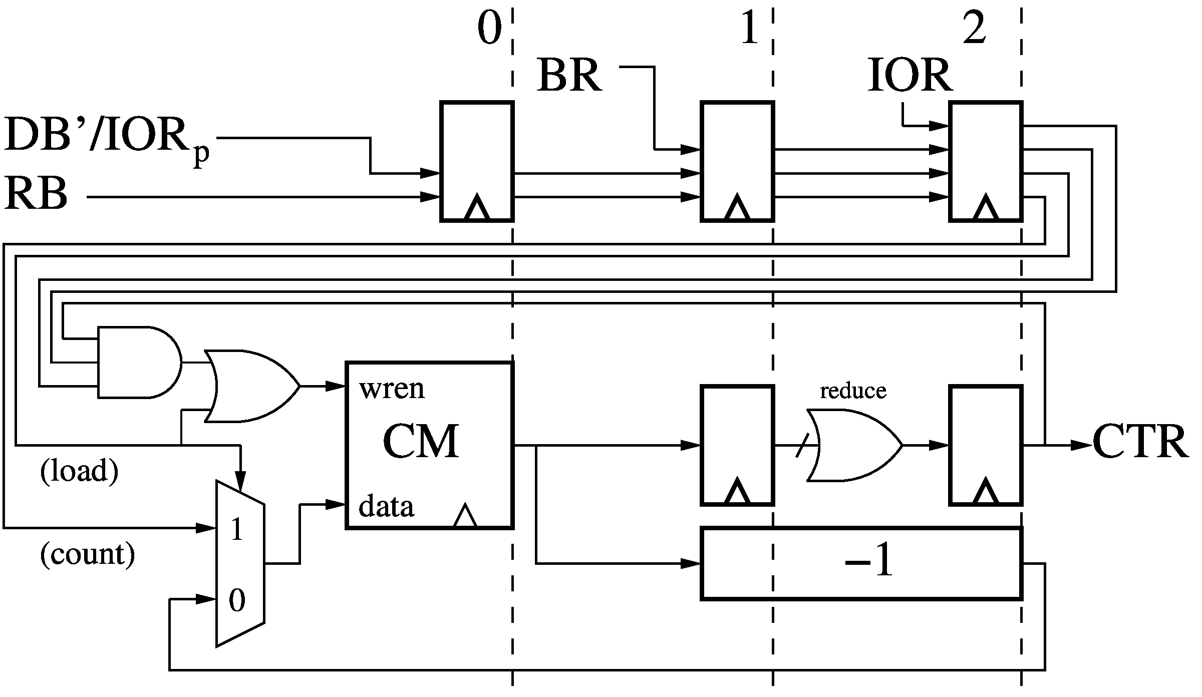 The 3-stage Branch Counter (BC) receives the previous instruction results and
destination address (RB/DB'), the Branch Reached (BR) signal, and the I/O Ready
for the current and previous instruction (IOR/IORp), all delayed by
some pipeline stages to synchronized them to the current thread. The Branch
Counter contains a Counter Memory (CM) which holds one 36-bit counter value for
each thread. The output of CM is both OR-reduced to a Counter Active flag (CTR)
and decremented by 1 (over 2 pipeline stages, to meet timing). If a branch is
reached, and the counter is active, and the current instruction is not Annulled
(IOR is high), then the Counter Memory stores the decremented counter value,
until it reaches zero. The result of a previous instruction
(RB/DB'/IORp), if not Annulled, can reload the counter.
The 3-stage Branch Counter (BC) receives the previous instruction results and
destination address (RB/DB'), the Branch Reached (BR) signal, and the I/O Ready
for the current and previous instruction (IOR/IORp), all delayed by
some pipeline stages to synchronized them to the current thread. The Branch
Counter contains a Counter Memory (CM) which holds one 36-bit counter value for
each thread. The output of CM is both OR-reduced to a Counter Active flag (CTR)
and decremented by 1 (over 2 pipeline stages, to meet timing). If a branch is
reached, and the counter is active, and the current instruction is not Annulled
(IOR is high), then the Counter Memory stores the decremented counter value,
until it reaches zero. The result of a previous instruction
(RB/DB'/IORp), if not Annulled, can reload the counter.
Branch Arbiter (BA)
 The 1-stage Branch Arbiter (BA) takes in the output of all the Branch Modules
(BM) and filters them with a Priority
Arbiter (PA) to pass along only the highest priority taken branch. There
are two BMs in this diagram. The output Jump (J) is set if any Jump is set, and
the PA is also fed an extra lowest-priority signal if no Jump is set. The PA
outputs a one-hot bitmask of Jumps used to select the associated Cancel (C) and
Branch Destination (BD) signals. If no Jumps are taken, any Cancel signal is
passed through (since an untaken branch may cancel a parallel instruction), and
the BD is set to zero (no one-hot mux input at that index).
The 1-stage Branch Arbiter (BA) takes in the output of all the Branch Modules
(BM) and filters them with a Priority
Arbiter (PA) to pass along only the highest priority taken branch. There
are two BMs in this diagram. The output Jump (J) is set if any Jump is set, and
the PA is also fed an extra lowest-priority signal if no Jump is set. The PA
outputs a one-hot bitmask of Jumps used to select the associated Cancel (C) and
Branch Destination (BD) signals. If no Jumps are taken, any Cancel signal is
passed through (since an untaken branch may cancel a parallel instruction), and
the BD is set to zero (no one-hot mux input at that index).
Controller (CTL)
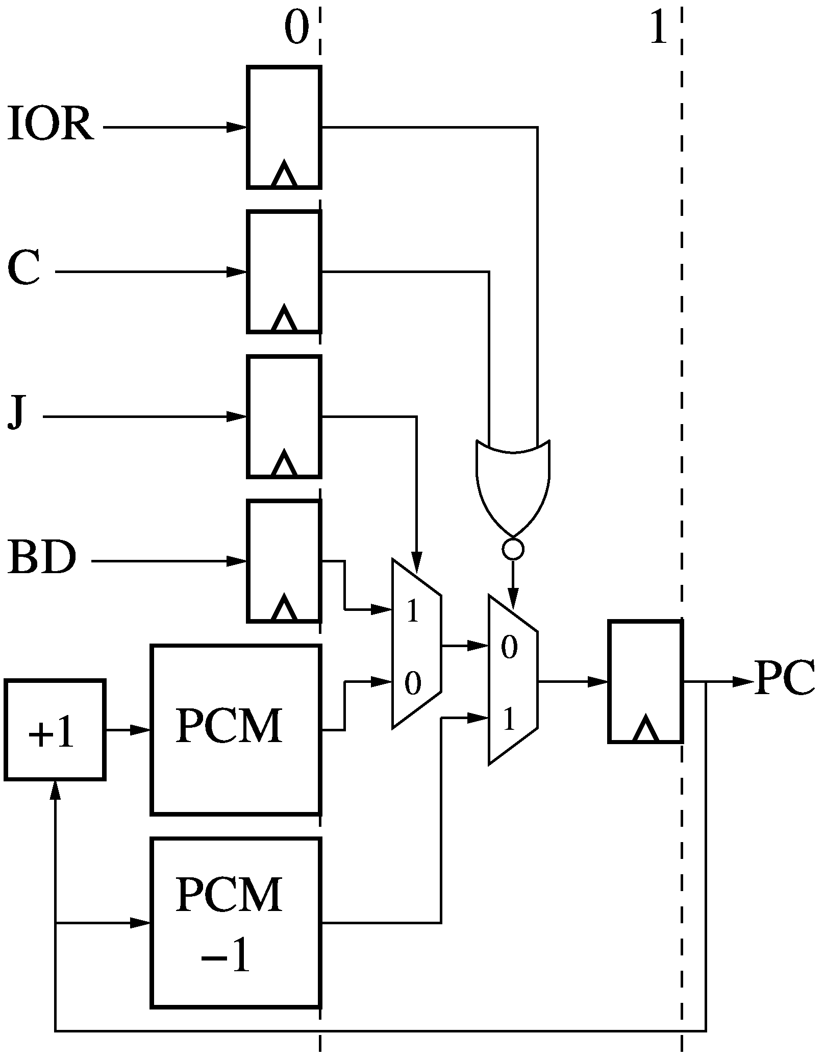 The 2-stage Controller (CTL) generates the next Program Counter (PC) value for
each thread based on any taken branch and if the instruction was Annulled.
There are two Program Counter Memories which store the next PC value (PCM) and
the current PC value (PCM -1) for each thread. If an instruction is Annulled
(IOR is high), the current thread PC value gets sent out again, re-trying the
same instruction. Cancel (C) overrides IOR, letting the next instruction be
fetched. If a branch is taken (Jump (J) is high), then the current PC takes
the value of the Branch Destination (BD).
The 2-stage Controller (CTL) generates the next Program Counter (PC) value for
each thread based on any taken branch and if the instruction was Annulled.
There are two Program Counter Memories which store the next PC value (PCM) and
the current PC value (PCM -1) for each thread. If an instruction is Annulled
(IOR is high), the current thread PC value gets sent out again, re-trying the
same instruction. Cancel (C) overrides IOR, letting the next instruction be
fetched. If a branch is taken (Jump (J) is high), then the current PC takes
the value of the Branch Destination (BD).
Address Splitter (AS)
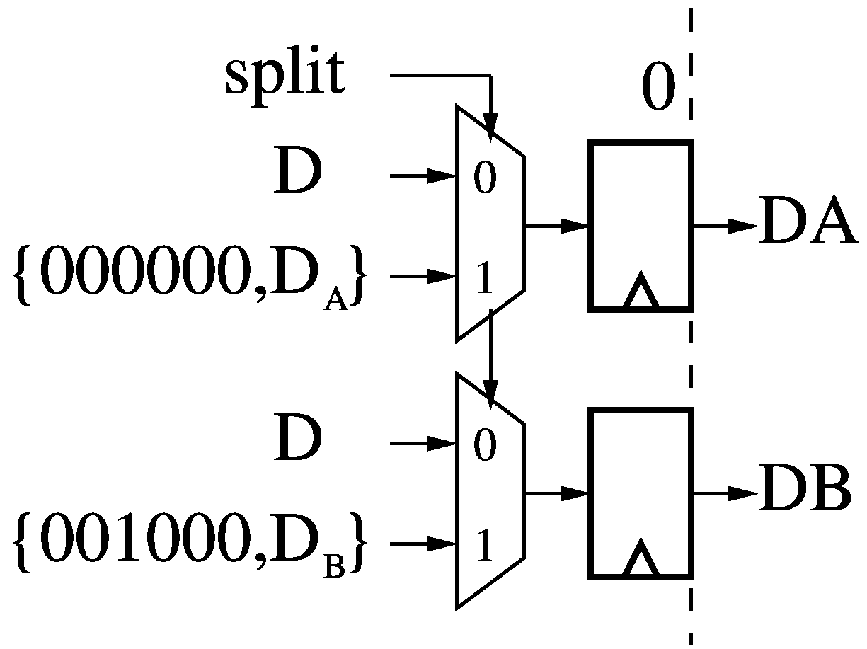 If the Control Bits (CTL, see Control Path) fetched by the opcode of the
current instruction have the Split bit set, then the instruction splits the
12-bit destination operand (D) into two 6-bit destinations (DA and DB), with
the necessary six most-significant bits to offset the destination into the
address space of the A (0-1023) and B (1024-2047) Data Memories (see Data
Path). Otherwise, D is simply replicated into DA and DB.
If the Control Bits (CTL, see Control Path) fetched by the opcode of the
current instruction have the Split bit set, then the instruction splits the
12-bit destination operand (D) into two 6-bit destinations (DA and DB), with
the necessary six most-significant bits to offset the destination into the
address space of the A (0-1023) and B (1024-2047) Data Memories (see Data
Path). Otherwise, D is simply replicated into DA and DB.
I/O Predication (PR)
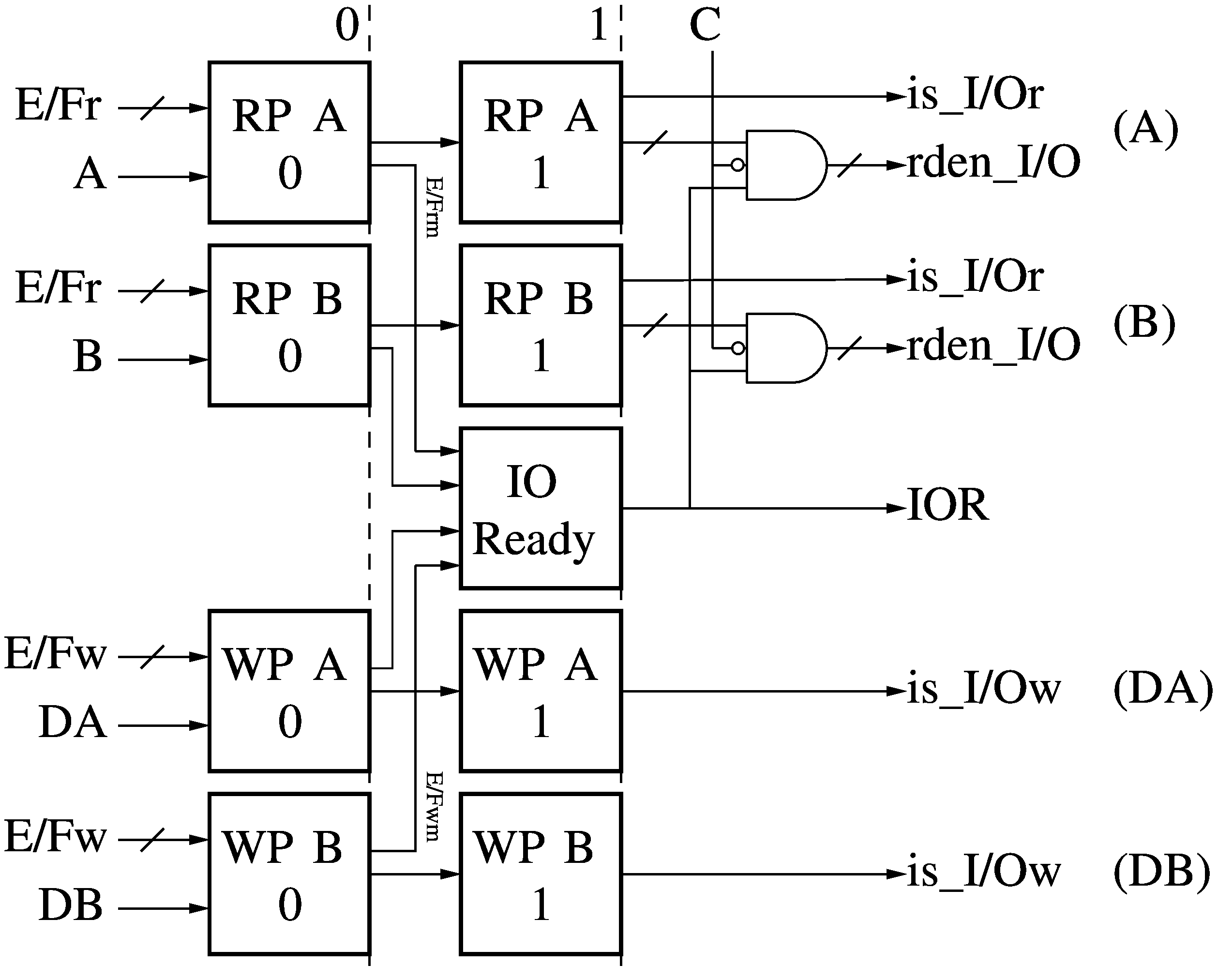 The 2-stage I/O Predication (PR) module receives the source and destination
operands from the current instruction (A, B, DA, DB) and the empty/full bits
from each read and write I/O port (E/Fr, E/Fw) and signals if each operand is
referring to an I/O port (I/Or, I/Ow) rather than Data Memory (DM). For the I/O
read ports, the read enable bit for the active port, if any, is also raised
(rden_I/O). The equivalent write enable signals for the I/O write ports
(I/Ow_wren) are created later in the Memory Write (MW) module. The
all-important I/O Ready (IOR) signal is generated here, based on the masked
empty/full bits (E/Frm and E/Fwm). The read enable signals (rden_I/O) are gated
by IOR or by the Cancel (C) signal from the Flow Control module (FC), so if the
current instruction is Annulled or Cancelled, no I/O port operation takes
place. The I/O write enable signals (I/Ow_wren) are gated in the same manner
later, in the Memory Write module (MW).
The 2-stage I/O Predication (PR) module receives the source and destination
operands from the current instruction (A, B, DA, DB) and the empty/full bits
from each read and write I/O port (E/Fr, E/Fw) and signals if each operand is
referring to an I/O port (I/Or, I/Ow) rather than Data Memory (DM). For the I/O
read ports, the read enable bit for the active port, if any, is also raised
(rden_I/O). The equivalent write enable signals for the I/O write ports
(I/Ow_wren) are created later in the Memory Write (MW) module. The
all-important I/O Ready (IOR) signal is generated here, based on the masked
empty/full bits (E/Frm and E/Fwm). The read enable signals (rden_I/O) are gated
by IOR or by the Cancel (C) signal from the Flow Control module (FC), so if the
current instruction is Annulled or Cancelled, no I/O port operation takes
place. The I/O write enable signals (I/Ow_wren) are gated in the same manner
later, in the Memory Write module (MW).
I/O Read Predication (RP)
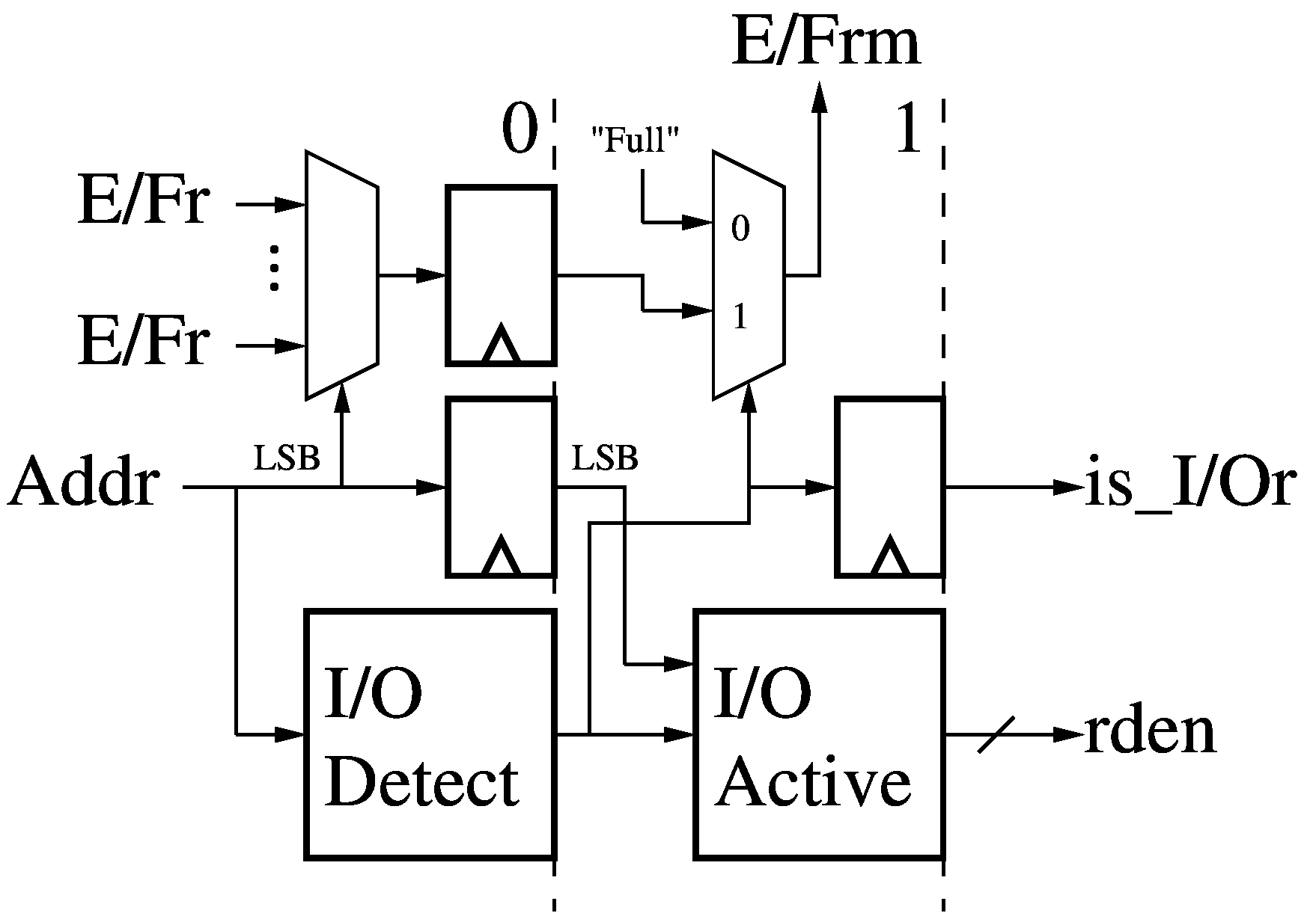 The 2-stage I/O Read Predication (RP) module receives a read address (Addr) for
a Data Memory (DM) and the empty/full bits (E/Fr) for any I/O read ports mapped
in that Data Memory space. The translated least-significant bits of the
address select an empty/full bit, while the whole address is decoded to determine if it refers to an I/O
port. If the address refers to an I/O read port, we pass on the corresponding
empty/full bit, else we mask it with a "Full" signal since memory is always
ready (E/Frm). Finally, we signal if this read accesses I/O (is_I/Or) and raise
the read enable (rden) line for the accessed I/O port, if any.
The 2-stage I/O Read Predication (RP) module receives a read address (Addr) for
a Data Memory (DM) and the empty/full bits (E/Fr) for any I/O read ports mapped
in that Data Memory space. The translated least-significant bits of the
address select an empty/full bit, while the whole address is decoded to determine if it refers to an I/O
port. If the address refers to an I/O read port, we pass on the corresponding
empty/full bit, else we mask it with a "Full" signal since memory is always
ready (E/Frm). Finally, we signal if this read accesses I/O (is_I/Or) and raise
the read enable (rden) line for the accessed I/O port, if any.
I/O Write Predication (WP)
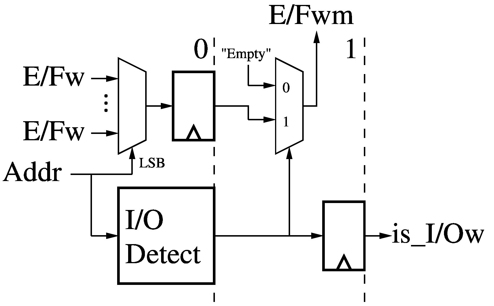 The 2-stage I/O Write Predication (WP) module receives a write address (Addr)
for a Data Memory (DM) and the empty/full bits (E/Fw) for any I/O write ports
mapped in that Data Memory space. The translated least-significant bits of the
address select an empty/full bit, while the whole address is decoded to determine if it refers to an I/O
port. If the address refers to an I/O write port, we pass on the corresponding
empty/full bit, else we mask it with an "Empty" signal since memory is always
ready (E/Fwm). Finally, we signal if this write accesses I/O (is_I/Ow). The
I/O port write enable signals (I/Ow_wren) are generated later in the Data
Memory (DM).
The 2-stage I/O Write Predication (WP) module receives a write address (Addr)
for a Data Memory (DM) and the empty/full bits (E/Fw) for any I/O write ports
mapped in that Data Memory space. The translated least-significant bits of the
address select an empty/full bit, while the whole address is decoded to determine if it refers to an I/O
port. If the address refers to an I/O write port, we pass on the corresponding
empty/full bit, else we mask it with an "Empty" signal since memory is always
ready (E/Fwm). Finally, we signal if this write accesses I/O (is_I/Ow). The
I/O port write enable signals (I/Ow_wren) are generated later in the Data
Memory (DM).
I/O Ready (IOR)
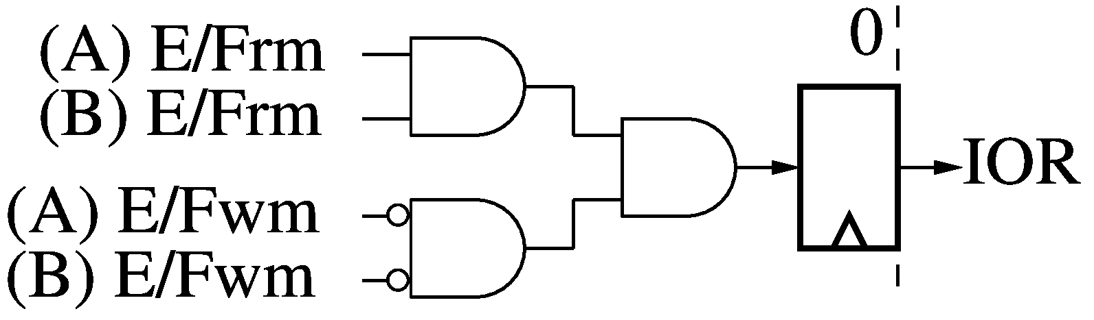 The I/O Ready module (IOR) takes in the masked read/write empty/full bits
(E/Frm and E/Fwm) for both the A and B Data Memories (DM). If all the
empty/full read bits are "Full" (logic 1), and all the empty/full write bits
are "Empty" (logic 0), then we raise I/O Ready (IOR) to signal the rest of the
system that all I/O ports referenced by an instruction are ready and thus the
instruction (and any parallel address offsets and branch operations) may
proceed. If IOR is low, the instruction is "Annulled": it is converted to a
no-op and re-fetched the next time the thread comes around. Any side-effects
(e.g.: decrementing loop counters or post-incrementing address offsets) are
also prevented.
The I/O Ready module (IOR) takes in the masked read/write empty/full bits
(E/Frm and E/Fwm) for both the A and B Data Memories (DM). If all the
empty/full read bits are "Full" (logic 1), and all the empty/full write bits
are "Empty" (logic 0), then we raise I/O Ready (IOR) to signal the rest of the
system that all I/O ports referenced by an instruction are ready and thus the
instruction (and any parallel address offsets and branch operations) may
proceed. If IOR is low, the instruction is "Annulled": it is converted to a
no-op and re-fetched the next time the thread comes around. Any side-effects
(e.g.: decrementing loop counters or post-incrementing address offsets) are
also prevented.
Addressing Module (AD)
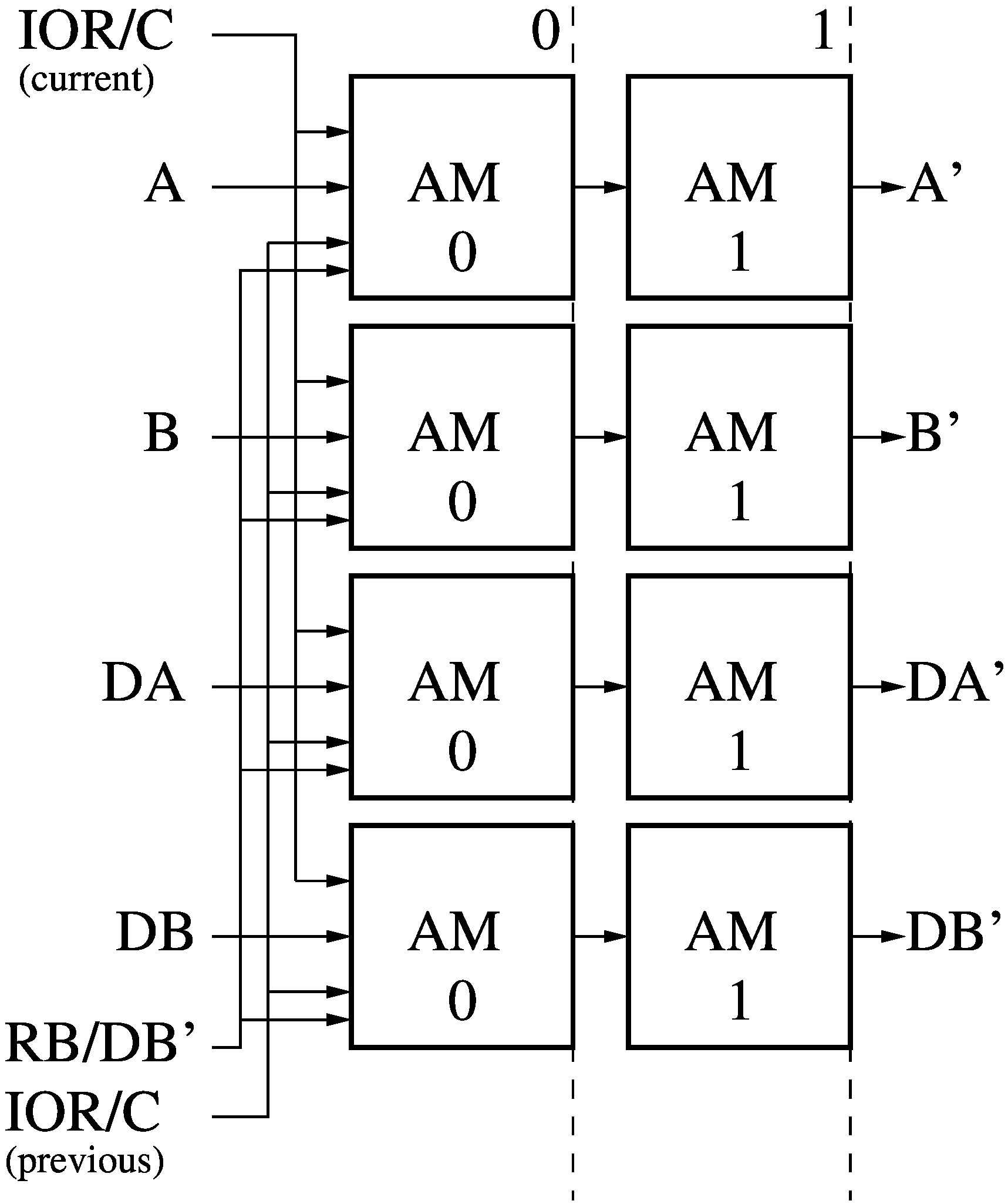 The Addressing module (AD) simply groups four Address Modules (AM)
which each modify a raw address from the instruction operands (A, B, DA,
DB) into offset versions (A', B', DA', DB').
The Addressing module (AD) simply groups four Address Modules (AM)
which each modify a raw address from the instruction operands (A, B, DA,
DB) into offset versions (A', B', DA', DB').
Address Module (AM)
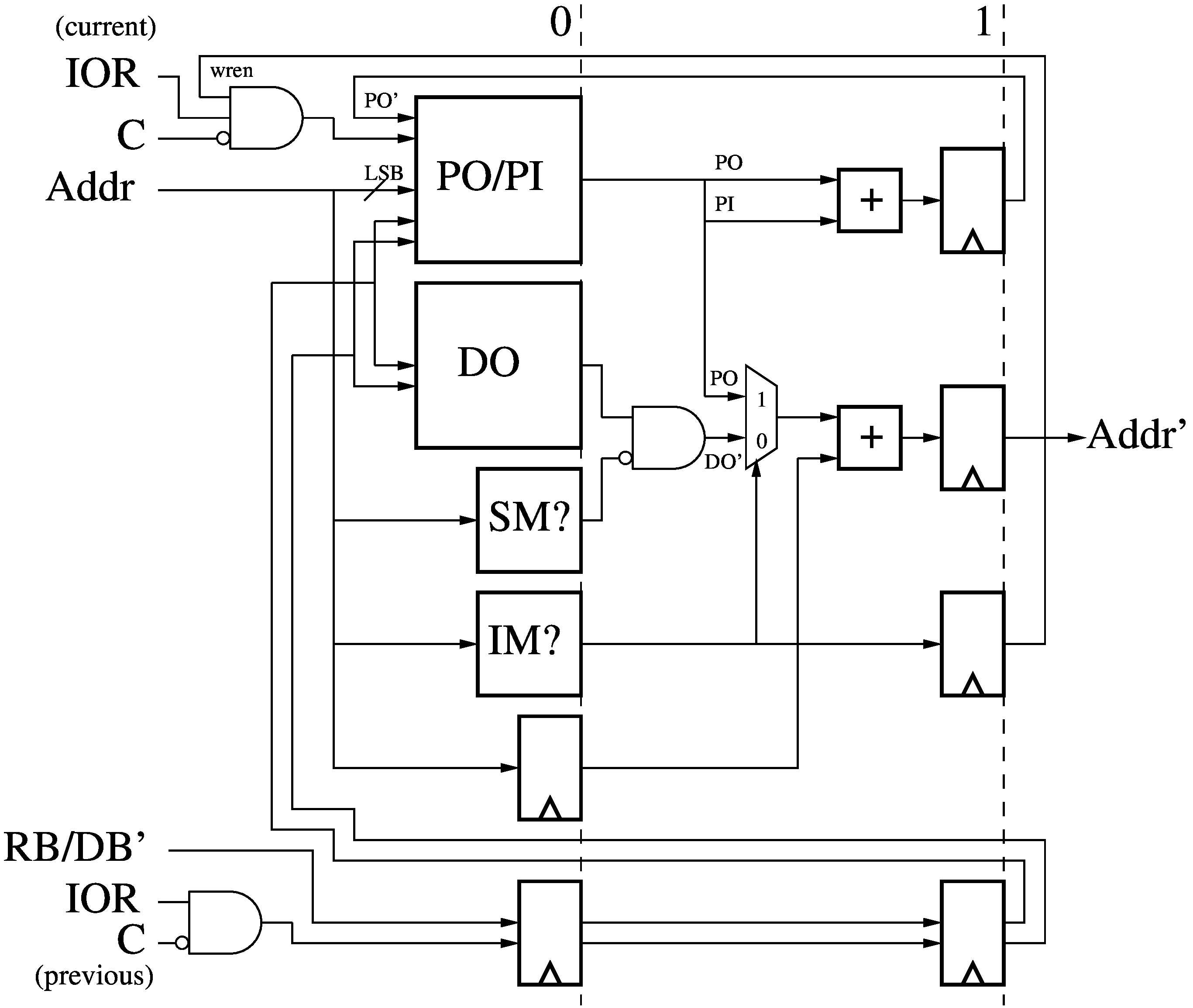 The 2-stage Address Module (AM) receives an address (Addr) and then adds a
per-thread offset to it (Addr'). The (translated) least-significant bits of the
address index into Programmed Offset (PO) and Programmed Increment (PI) tables.
The whole address is decoded to see if it falls in the range of Shared Memory
(SM?) and Indirect Memory (IM?), as well as carried along to the next pipeline
stage.
The 2-stage Address Module (AM) receives an address (Addr) and then adds a
per-thread offset to it (Addr'). The (translated) least-significant bits of the
address index into Programmed Offset (PO) and Programmed Increment (PI) tables.
The whole address is decoded to see if it falls in the range of Shared Memory
(SM?) and Indirect Memory (IM?), as well as carried along to the next pipeline
stage.
- By default, a per-thread Default Offset (DO) is added to the address, which
relocates accesses to that threads' allocated memory range.
- If the address refers to a Shared Memory location, then the Default Offset
is masked to zero, making that physical location shared by all threads. Shared
memory locations include the literal pool, the I/O ports, High Memory, and
Instruction Memory.
- If the address refers to an Indirect Memory location, then a Programmed
Offset is added to the address, acting as a pointer to redirect the access to
anywhere else in the address space. Indirect Memory overrides Shared Memory.
If the address refered to an Indirect Memory location, then the Programmed
Offset is post-incremented with the Programmed Increment and stored back into
its table entry (PO'), unless the current instruction was Cancelled or
Annulled. The Programmed and Default Offset tables can be updated by the result
of a previous instruction (RB/DB') if not Cancelled or Annulled. The Shared
and Indirect memory ranges are hard-coded.
Data Memory Read (RD0/RD1)
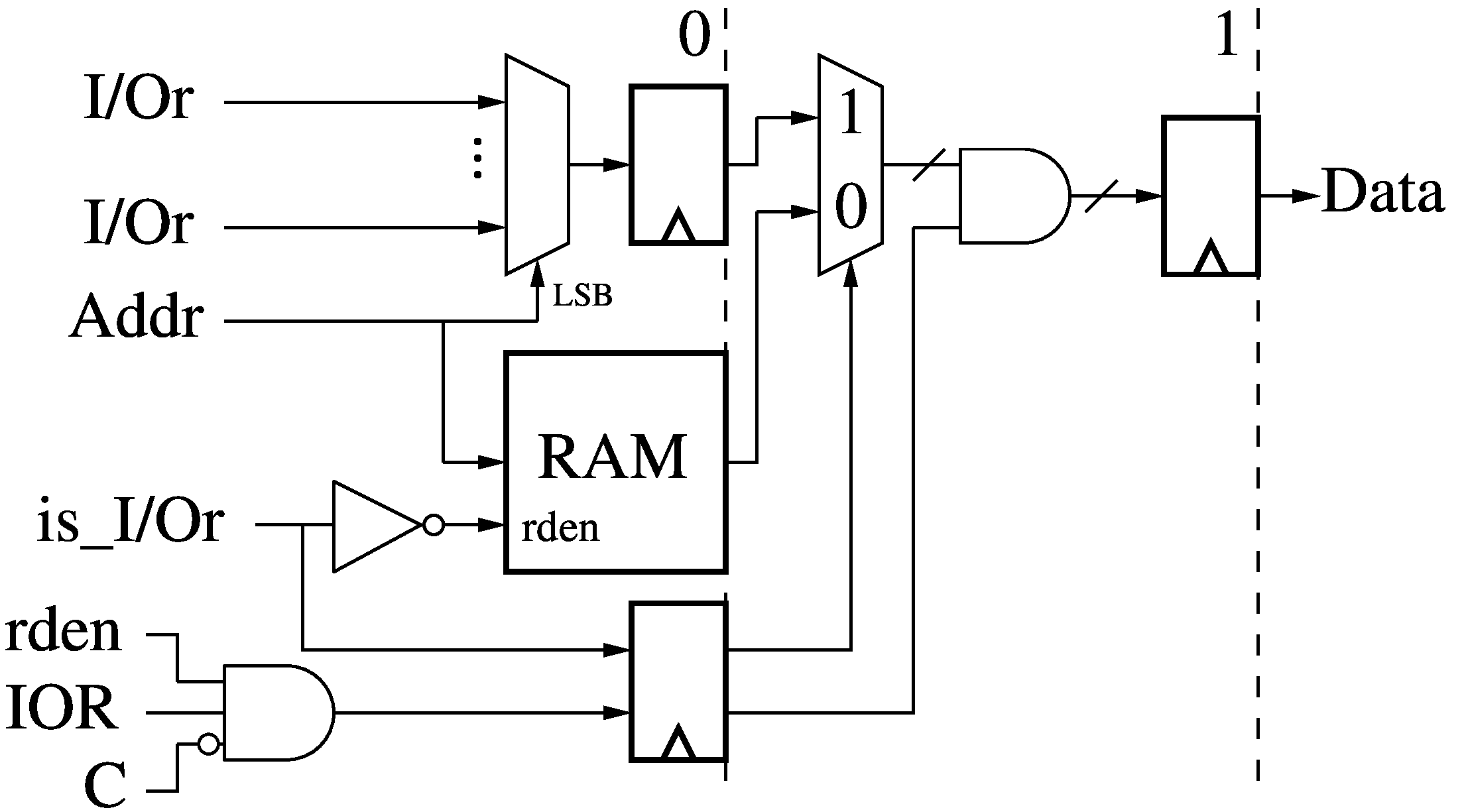 The 2-stage Data Memory Read (RD0/RD1) receives a read address (Addr) from an
instruction operands (A' or B') and the input from the I/O read ports (I/Or).
The least-significant bits of the address (after translation) select one of the I/O port,
while the full address reads from the data memory (RAM) if the address was not
previously determined in the I/O Predication module (PR) to be an I/O port
address (is_I/Or). Otherwise, the RAM read access is disabled and the input from the
selected I/O port is passed along instead. Finally, if a previously generated
read enable (rden) is not active, or if the instruction was Annulled or
Cancelled, the output (Data) is masked to zero.
The 2-stage Data Memory Read (RD0/RD1) receives a read address (Addr) from an
instruction operands (A' or B') and the input from the I/O read ports (I/Or).
The least-significant bits of the address (after translation) select one of the I/O port,
while the full address reads from the data memory (RAM) if the address was not
previously determined in the I/O Predication module (PR) to be an I/O port
address (is_I/Or). Otherwise, the RAM read access is disabled and the input from the
selected I/O port is passed along instead. Finally, if a previously generated
read enable (rden) is not active, or if the instruction was Annulled or
Cancelled, the output (Data) is masked to zero.
Data Memory Write (WR0/WR1)
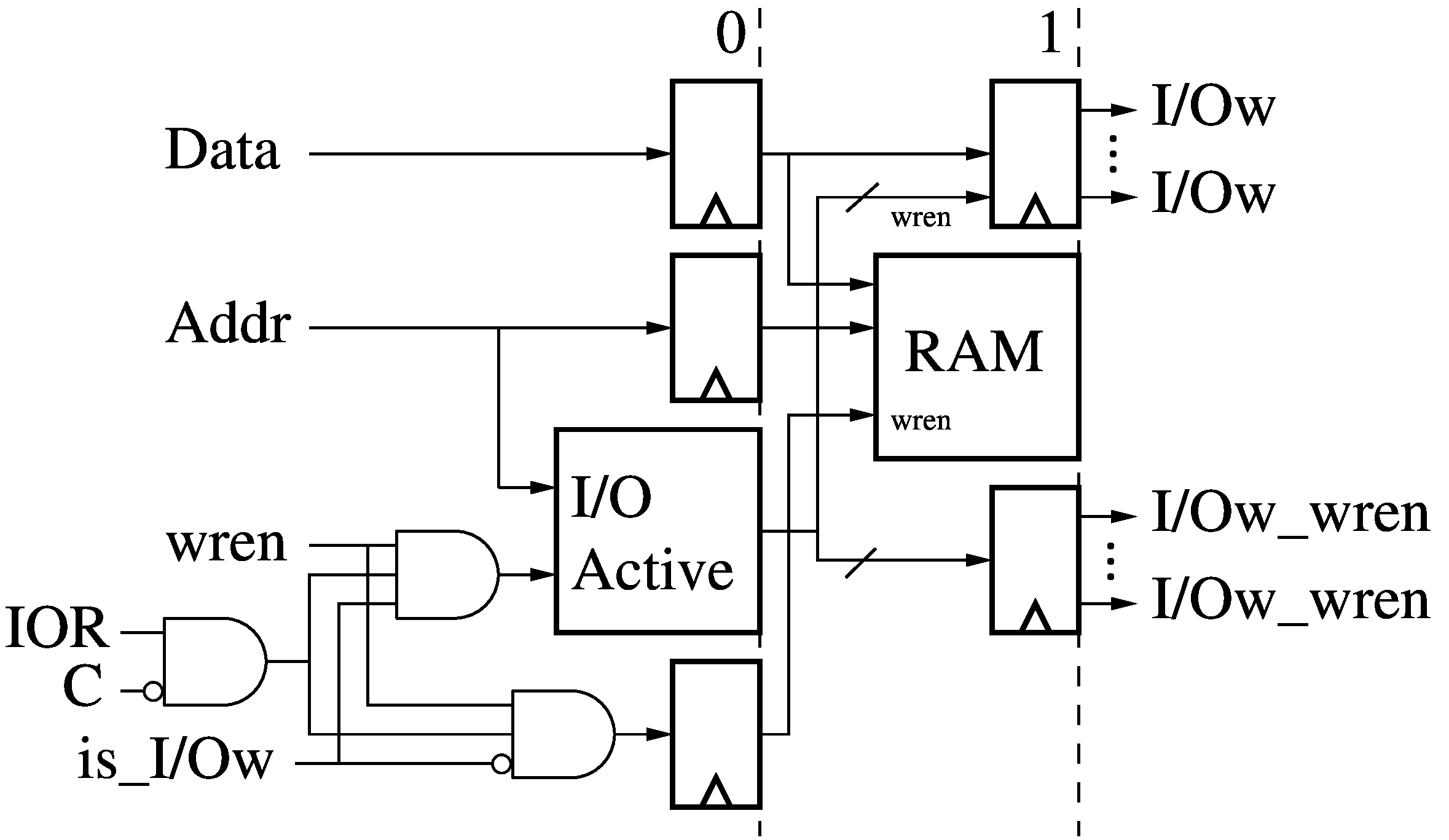 The 2-stage Data Memory Read (WR0/WR1) receives a write address (Addr, from DA'
or DB') and data (Data, from RA or RB) from the current instruction as well as
a previously generated write enable (wren) and the signal from the I/O
Predication module (PR) which indicates if the address is accessing an I/O port
(is_I/Ow). If the address is not referring to an I/O port, nor Cancelled or
Annulled, then the data is written to the data memory (RAM). Otherwise, a
signal is raised for the referenced I/O port and the write data is written to
that referenced I/O port (I/Ow), and its associated write enalbe (I/Ow_wren) is
raised.
The 2-stage Data Memory Read (WR0/WR1) receives a write address (Addr, from DA'
or DB') and data (Data, from RA or RB) from the current instruction as well as
a previously generated write enable (wren) and the signal from the I/O
Predication module (PR) which indicates if the address is accessing an I/O port
(is_I/Ow). If the address is not referring to an I/O port, nor Cancelled or
Annulled, then the data is written to the data memory (RAM). Otherwise, a
signal is raised for the referenced I/O port and the write data is written to
that referenced I/O port (I/Ow), and its associated write enalbe (I/Ow_wren) is
raised.
Arithmetic and Logic Unit (ALU)
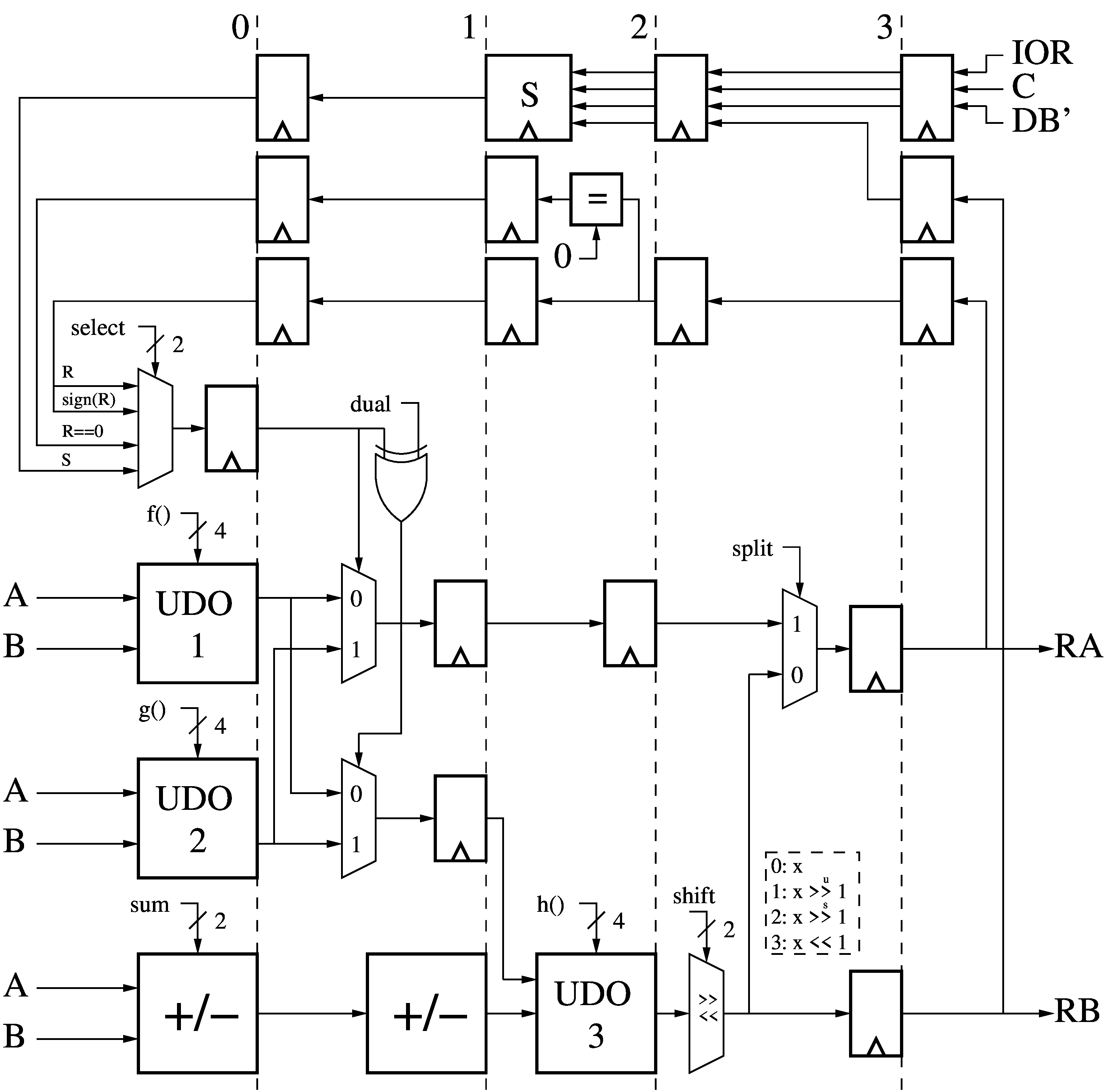 The 4-stage Arithmetic and Logic Unit (ALU) receives the 36-bit A and B data
words from the Data Memory (DM), the 20-bit control bits from the Opcode
Decoder Memory (OD), and the 12-bit destination address DB'.
The control bits are divided into multiple fields:
The 4-stage Arithmetic and Logic Unit (ALU) receives the 36-bit A and B data
words from the Data Memory (DM), the 20-bit control bits from the Opcode
Decoder Memory (OD), and the 12-bit destination address DB'.
The control bits are divided into multiple fields:
- select, 2 bits, which chooses one of:
- the previous instruction result (R),
- a stored previous result (S),
- a word-wide all-ones bit-mask set from the sign bit of R (sign(R)) or whether is it zero (R==0).
- f() and g(), both 4 bits, which define one of
the 16 possible dyadic Boolean operation on A and B. The output of "select"
does a bit-wise interleaving of the outputs of f() and g(), creating a triadic Boolean operator.
- dual, 1 bit, which inverts one of the f()/g() output selections, allowing
us to pick the other alternative defined by "select".
- sum, 2 bits, which selects one of the four possible addition/subtraction of
A and B: +/-A+/-B.
- h(), 4 bits, which defines a Boolean combination of the outputs of f() and
g(), and of "sum".
- shift, 2 bits, which shifts the output of h() by zero bits, or one bit
left, or one bit right signed or unsigned.
- split, 1 bit, which either copies the output of "shift" to both outputs (RA
and RB), or splits them such that RA gets a Boolean combination of A and B, and
RB gets the result of an arithmetic (and maybe also Boolean) operation on A and
B.
The RA output gets fed back to the ALU, after another 4 cycles of delay to
synchronize it to the next instruction of the same thread, and becomes R and
its derived flags. Similarly, if the previous instruction's destination address
(DB') referred to the S register, and was not Annulled or Cancelled, then the
ALU result RB is also synchronized to the next thread instruction and saved in
S, where it persists. Thus we can perform Boolean operations on A, B, and the
result of a previous instruction.
Depending on the control bits and the values
of R and S, this ALU can compute all the usual dyadic Boolean operations and
addition/subtractions of A and B, and more complex combinations thereof:
- All operations of the forms a◊(+/-b+/-c), where
"◊" denotes any one possible dyadic Boolean operation. These cover all the
basic operations (Chapter 2, Basics) in Henry S. Warren's Hacker's Delight, which decribes
many algorithms built from such bit-parallel operations.
- Any Boolean operation involving A, B, and R/S as a single-step triadic Boolean operation. This halves the
number of steps when performing chains of Boolean operations, and executes more
complex operations such as majority/minority/carry in one step.
- Moving both A and B to RA and RB, optionally swapping bits between them
depending on the contents of R or S. This basic split mode allows moving two
data words at once when data movement dominates data computation. It is also
possible to do limited computation in the split mode, such as moving R to RA,
while outputting A or B plus 1 to RB, and having the destination addresses (DA
and DB) point to I/O ports, thus having these two values act as the data and
post-incrementing address for an external memory write.
Publications
- High-Speed Soft-Processor Architecture for FPGA Overlays
Thesis, Doctor of Philosophy (ECE), University of Toronto, 2014
Everything below, plus some background, work on expanded address spaces, instruction I/O predication, and benchmarking.
Slides: PDF
- Microarchitectural Comparison of the MXP and Octavo Soft-Processor FPGA Overlays
Charles Eric LaForest, Jason H. Anderson
ACM Transactions on Reconfigurable Technology and Systems (TRETS), May 2017, Volume 10, Issue 3, Article No. 19
Compares the micro-architecture, performance, and area of two
soft-processor FPGA overlays: the Octavo multi-threaded soft-processor and the
MXP soft vector processor, both compared against hardware implementations of
micro- benchmarks written in C synthesized with the LegUp HLS tool and also
written in the Verilog HDL. Overall, Octavo's higher operating frequency and
MXP's more efficient code execution results in similar performance from both,
within an order of magnitude of hardware implementations, but with a penalty
of an order of magnitude greater area.
- Approaching Overhead-Free Execution on FPGA Soft-Processors
Charles Eric LaForest, Jason Anderson, J. Gregory Steffan
IEEE International Conference on Field-Programmable Technology (FPT), December 2014, Shanghai, China
Describes the Branch Trigger and Address Offset Modules which can eliminate branching and addressing overheads, giving better performance than loop unrolling even against an "ideal" impossible reference processor.
Slides: PDF (also available from http://wiki.tcfpga.org/FPT2014 along with many others)
- Maximizing Speed and Density of Tiled FPGA Overlays via Partitioning
Charles Eric LaForest and J. Gregory Steffan
IEEE International Conference on Field-Programmable Technology (FPT), December 2013, Kyoto, Japan
Demonstrates simple design partitioning techniques to preserve performance when replicating datapaths ("tiling") via SIMD or multi-core scaling.
Slides: PPTX PDF
- Octavo: An FPGA-Centric Processor Family
Charles Eric LaForest and J. Gregory Steffan
ACM International Symposium on Field-Programmable Gate Arrays (FPGA), February 2012, Monterey, CA.
Describes the basic Octavo architecture, and how to maximize pipelined logic speed via "self-loop characterization".
Slides: PPTX PDF
fpgacpu.ca